3/30/2000
“Large” (8 x 9 inch) 1152 MHz Surplus Qualcomm RF/Synthesizer Board Conversion
Notes
by Ed Munn, W6OYJ, based on smaller 1152 board conversion by Kerry Banke,
N6IZW and
Chuck Houghton, WB6IGP.
The board has high harmonic content radiation and makes an excellent marker through
10368 Mhz.
Harmonics fall exactly at 2304, 3456, 5760, 10368, and 24192 Mhz.
If you enable U-21 as an
amplifier for LO Purposes, you can get +10 dBm output
of 1152 Mhz as LO for a 1296 Transverter.
The following description assumes you
view the component side with the 10 Mhz reference oscillator
at center right
and power connector on lower left edge.
Low level synthesized output is at TP1 - can replace the connector with an SMA.
U19 originally is an active upconverter. Has poor performance at 1296 output due
to high LO feedthru
- but is ok for 900 Mhz output.
U22 is an active downconverter - I.F. output from pin 5 - Works ok at 900-1296 input and 144 Mhz IF
See the diagrams of the U-1 synthesizer IC to locate the pins. The dot at top
center is Pin # 1.
Numbers go counter clockwise, Pin#6 is left edge of top, Pin#7
is top of left side and Pin #17 is
bottom of left side, Pin#18 is left end of
bottom and # 28 is right of bottom, etc.
To change U-1 synthesizer for 1152 Mhz VCO output, you will need to carefully
cut U-1 Pins #2, 5,
19, and 22 at the pcb pads with a sharp pointed (X-Acto)
knife, and gently lift the IC leads up away
from the pcb. As they are internally
pulled “high” this raises them to the “1” state.
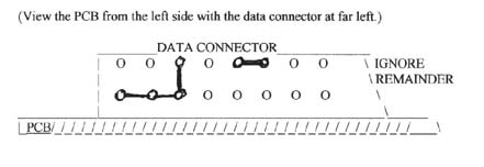
Next you need to ground Pins #7, 9, 10, and 16. This is very easy to accomplish
because on this board
they are brought directly out to the black data connector
J-1 on the upper left side of the PCB. Solder
the connector pins as shown below
to accomplish this.
This board does not have a VCO/2 divider as do the boards we use for conversion
to higher microwave
bands. The synthesizer programming solution for this VCO
to produce 1152.000 output is:
N=1152, M=114, A=2, and R=9.
The internal PLL reference frequency must be set to 1 MHz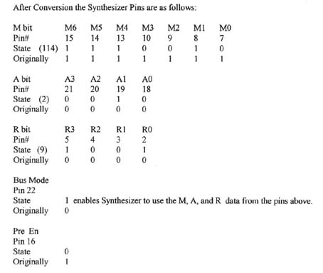
Original VCO range is about 750-1000 Mhz. To increase VCO range to 1152 Mhz, solder
a 1000 pF
chip cap to ground the midpoint of the PCB loop inductor below Q3.
(just below center screw hole at
top of board, where the Q3 symbol is). See separate
diagram.
The 10 Mhz reference osc adjustment is accessed by removing the unneeded FL2.
Use a Vise Grip
wrench to wiggle it back and forth until metal fatigue occurs.
U2 and U4 , just below the synthesizer chip must be removed as they connect to
the programming
inputs of the synthesizer. A sharp knife can be used to cut the
IC leads close to the body of the ICs and
then pry with the knife to lift them
off the board.
The Red LED DS1, above the syn chip is a no lock indicator - Normally it will be off.
The J4 reference connector has the 10 Mhz reference output (TNC connector)
The J3 IF (TNC) connector is connected through a filter to a splitter and then
to the up and down
converters. It also has +15 VDC present. Remove L56 to remove
DC from J3.
With these changes, the board works as a stand alone low level marker. To enable
U-21 as an
amplifier for higher (+10 dBm) output or as an upconverter amplifier,
do the following:
Ground the end of R62 nearest the top board edge to turn on U21 & upconverter power.
To use board for 1152 LO high level output only, remove U19 with a sharp knife
and jumper the pcb
pads for U19-1 to U19-5 (provides path for LO). See the attached
diagram. Then jumper across the
microstrip filter about 1.5 inches to right of
top center mounting hole. (emerges under L42 toward
input to U21). I soldered
a #18 bus wire from the beginning of the filter next to L42, across the filter,
making
solder contact with the filter all the way to the left end of C148, the input to
U-21. I then
soldered an SMA connector body to the ground plane just above and
to the right of C-149, with its
center lead to the right end of C149. This is
the new LO Output connector.
If you don’t get enough output you can cut the microstrip just to the right of your connection to C149.
If you decide to use the PCB as a downconverter for 900 or 1296 Mhz, or an upconverter
for 900 Mhz,
you can omit the SMA connector installation. The output microstrip
filter on the right edge near top
may be ok to leave in as center freq is about
1.1 GHz. If the I.F output at J-3 is inadequate then jumper
across the output
filter.
The large boards have a power connector along the lower left side. This is J2.
Power connections are:
GND to Pin #1, +5VDC @ 0.5 A to Pin #6 and jumper also
to Pin#15, +15 VDC @ 120 mA to Pin
#4..