12/3/2009 (Revised and added Paragraph 11 with Antenna orientation and Photos
of assembled ODU
5/2/07 (Revised Paragraphs 7, 8 and pwr distribution schematic
in Paragraph 10)
11/30/05 (Revised Paragraphs 4B, 6, 10)
9/2/03 (Revised Paragraphs
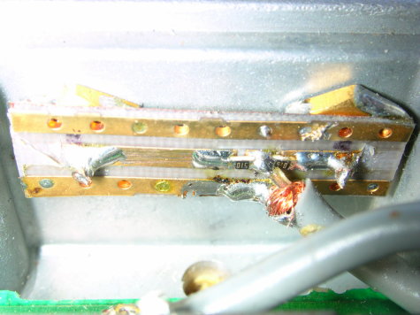
4B, 5A, 6 and 10)
Modification of the Pcom 23 GHz "High Side LO" ODU
as a 24 GHz Transverter
Status Report by Kerry Banke, N6IZW.
Web pages by Ed
Munn, W6OYJ
1. At one of the last SBMS meetings attended by Sam Luitwieler, K6VLM, he said that although he had modified two of the low side LO Pcom ODUs to 24 GHz, he felt that the high side LO units would be easier to modify. His reason was that the required LO inputs to the Tx and Rx modules would be closer to the original frequencies used, and less re-tuning would be required to reach the amateur 24 GHz band. Unfortunately Sam became a silent key before he could expand on this approach. More recently, Kerry Banke, N6IZW assisted by Chuck Houghton, WB6IGP have been working on an approach to modify the high side LO units. This approach does not use the original synthesizer portion of the Synthesizer Module, but instead produces a cleaner and more stable LO signal using a Qualcomm 2640 MHz DRO Synthesizer referenced by a separate 10 MHz TCXO. The remainder of the Pcom Synthesizer Module, including its X5 multiplier stages to 13,200 MHz, is used in this approach. Use of a 432 MHz i.f. Transceiver is assumed with the modified transverter, for operation on 24192 MHz.
2. The Pcom 23 GHz units come in two versions, one in which the millimeter wave LO signals applied to the Tx and Rx 1st mixers are below the intended operating frequencies, and the other in which the LO signals are above the operating frequencies. Thus the units are described as "Low Side" and "High Side" respectively. To tell the difference, view the external nameplate of the ODU and compare the indicated receiver frequency range to the transmitter frequency range. If the receiver range is higher than the transmitter range, the unit is a "High Side" LO version. Another way to check this is to remove the cylindrical cover exposing the internal modules. Then disconnect one of the two coax hard lines from the Synthesizer Module going to either the Rx or Tx Module. Connect the exposed SMA output of the synthesizer module to an external microwave frequency counter via enough attenuation to protect the counter from the approx. +20 dBm output. Apply Negative 48 volts (approx. 1.0 amps) to the Type "N" coax connector to activate the ODU. You should measure a signal in either the 9-10 GHz range or in the 12-13 GHz range. These signals are half the frequency of the millimeter wave LO frequencies applied to Tx and Rx front-end mixers. If your measurement result is in the 12-13 GHz range, you have a high side LO version of the ODU.
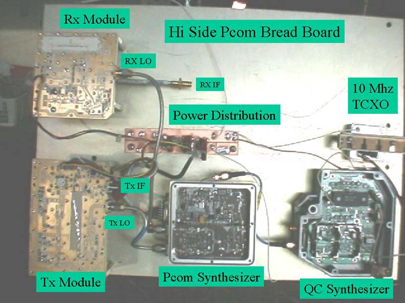
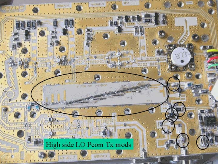
3. The following is a module-by-module account of comments made by Kerry Banke describing his modifications. In each case he prepared photos with labels showing the affected areas of the modules. Some of these photos will later be replaced with ones of better clarity, but the intent of this document is to indicate the current status of the modification approach. More changes are expected to arise as this process continues. At the end of the article you can see a photo of the assembled units mounted to the original dish Antenna Diplexer housing. Conceptual Block Diagrams of the Unmodified High Side ODU, and of the Modified ODU are shown here. Shown here is the breadboard layout Kerry used in evaluating these changes.
4A. Original IF Processor Module. This unit is not used and should be removed and set aside for possible later use of some parts and connectors.
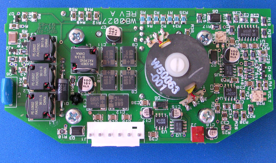
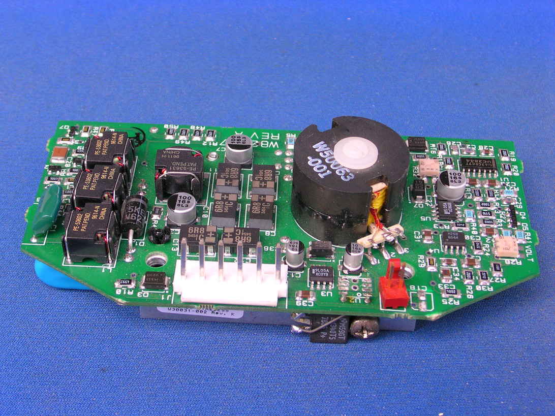
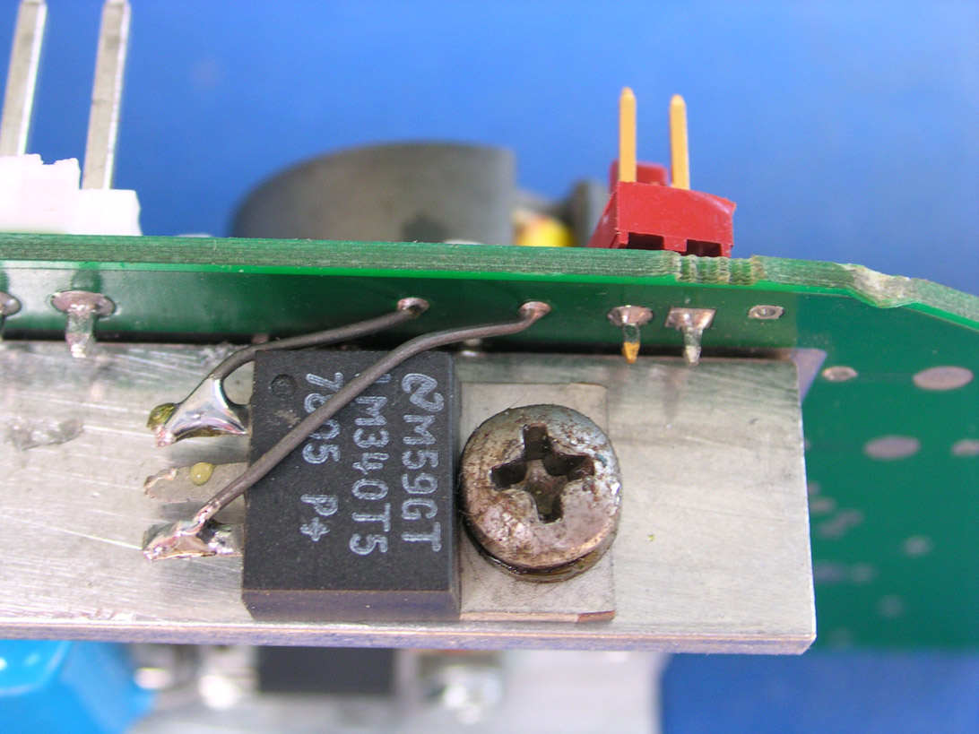
4B. Original Power Supply Module. (Revised 8 Sept 2005).
This module requires approx. Negative 48 volts at about 1.0 amps to power the ODU
in full duplex operation. Earlier modifications discarded the power supply module,
but current thinking is to make one change to the positive 5 volt regulator and use
the module. It provides all the voltages needed by the modified modules; regulated
+12 Volts dc, regulated +5 Volts dc, and regulated Negative 5 Volts dc bias. There
is no protection included for loss of the negative bias, and no T/R switching. These
are dealt with in a new separate module described in Paragraph 10.
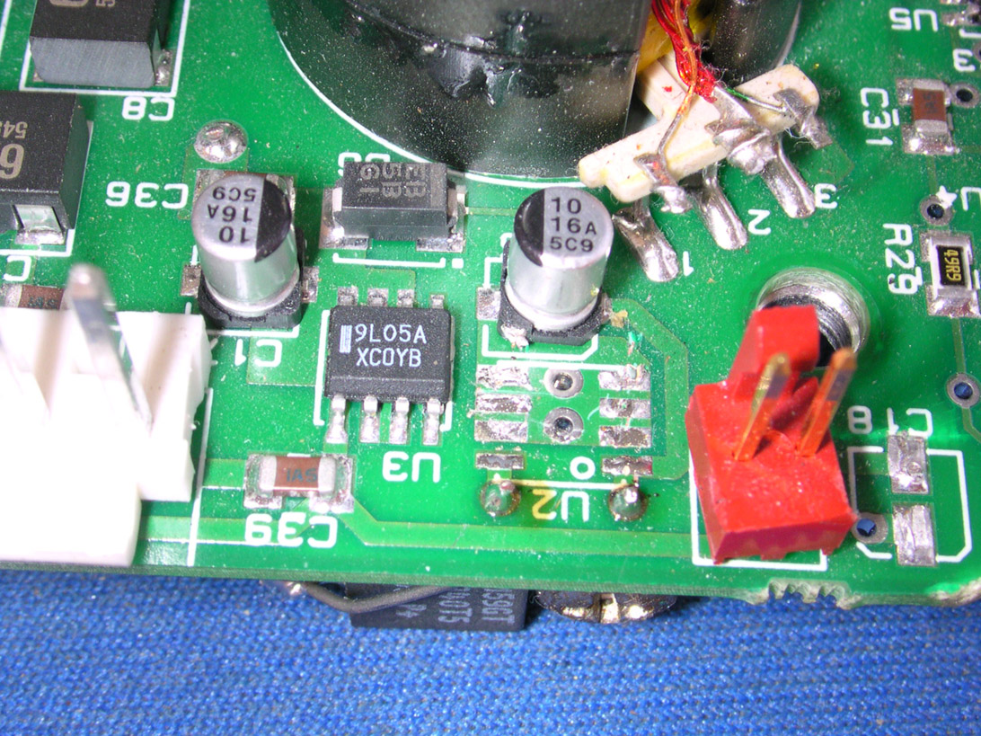
The change
required to the module is to remove the original positive 5 volt low-current regulator
IC (U2) and replace it with a higher current 7805 regulator. The photos show the
modified power supply module, a close up view
of the removed IC, and a view of the newly installed 7805
regulator.
An external DC/DC converter is used to generate the Negative 48
VDC from any +12VDC source. Tests indicate that the -48V input is not critical and
the power supply functions from as little as -30 VDC. W6OYJ is currently using a
12V to 36V dc/dc module available from a web vendor for about $12 including shipping
& handling. The pinouts for the Pcom power supply are: Pin 1 (white) -48V input,
Pin 2 (brown) Gnd, Pin 3 (red) +12VDC output, Pin 4 (yellow) +5VDC output, Pin 5
(green) -5V (bias) ourput, and Pin 6 (black) Ground.
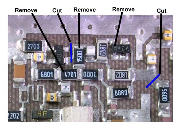
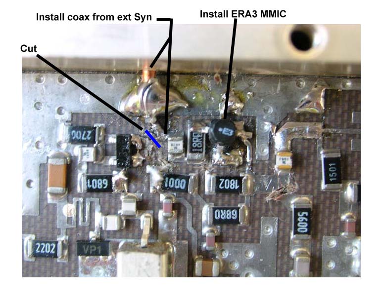
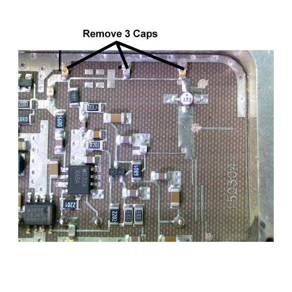
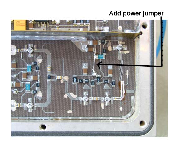
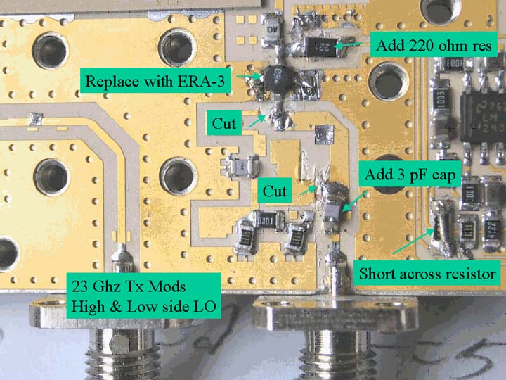
5. Modifying the Pcom Synthesizer Module. As mentioned above, the synthesizer portion of this Module is disabled in Step One by cutting traces and removing components. In Step Two, a new 2640 MHz input source to the VCO buffer stage is introduced via a coaxial line connected to one of the two outputs of the newly added separate Qualcomm DRO Synthesizer. Also in Step Two, the original VCO buffer stage is replaced with an ERA-3 MMIC to provide more gain. In Step Three, Remove three chip caps to increase the drive to the two X5 multipliers. No retuning of the X5 multiplier stages is needed in this High-Side LO modification. Their outputs provide ample (+20 dBm) LO/2 signal to drive the Tx and Rx Modules at 13,200 MHz. Finally in Step Four you add a power jumper in the lower right section of the module. The module power requirements are +12 Volts DC and Ground.
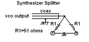
5A. Qualcomm DRO Synthesizer for 2640 MHz. This unit is described elsewhere and an internal splitter is added to it to provide separate outputs to the Synthesizer Module and the 2-3 GHz Up/Down Converter Module. See photo of the modified synthesizer with the splitter at the very top, the external view of the splitter, the pcb view, and the splitter circuit diagram. Each 2640 MHz output should provide about +5 dBm. The power requirements are +12 Volts DC and ground.
5B. Qualcomm 10.00 MHz TCXO reference oscillator. This is mounted near to, and provides its output to the Qualcomm DRO Synthesizer via a small coaxial lead. Its power requirements are +12 Volts DC and ground. For improved frequency stability an ovenized 10 MHz reference can be substituted.
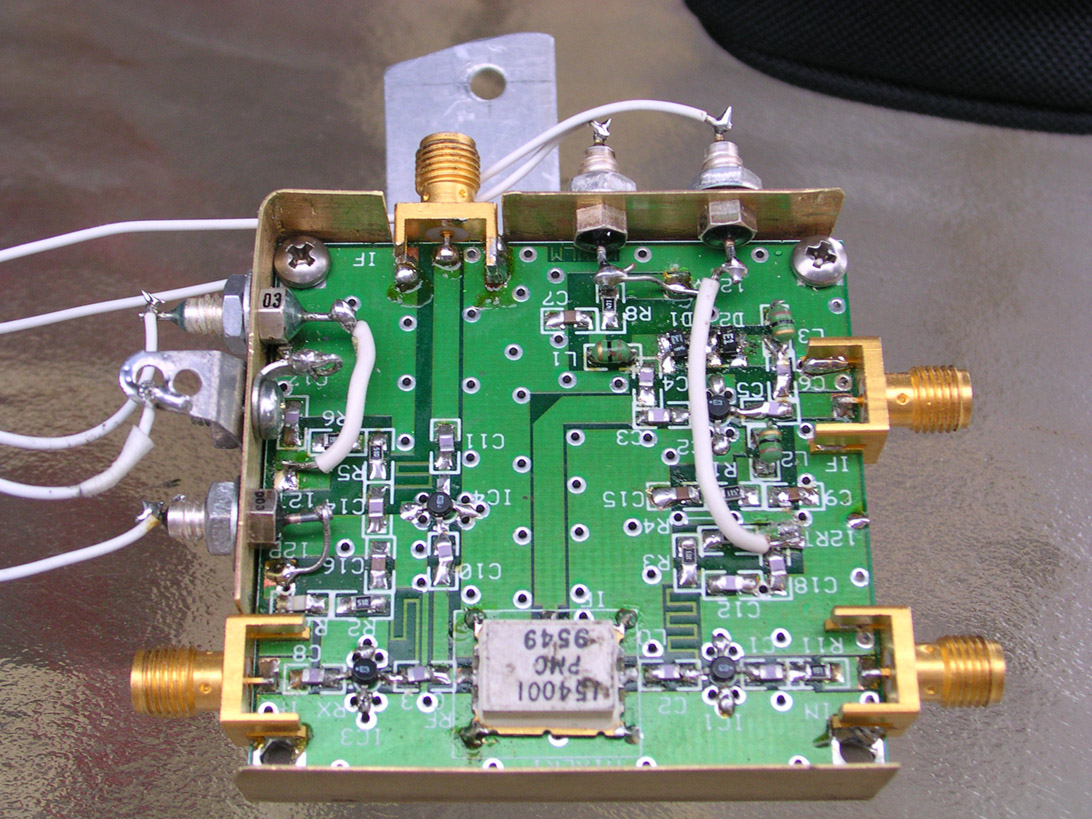
6. New 2-3 GHz Up/Down Converter Module. (Revised 8 Sept 2005.) Originally designed
by Sam, K6VLM with some recent modifications to accommodate component changes. This
is described elsewhere and sometimes has been called the "Mixer Board".
SBMS has a limited number of kits of this unit available to amateurs. It is more
than just a mixer, as it functions in either Up or Down direction as controlled by
the applied dc voltages, and includes gain stages and PIN Diode T/R switching. It
can operate over a range of RF inputs, including 2208 MHz for the high side LO units,
and the 3072 MHz required by the low side LO units. The i.f. input/output frequency
is 432 MHz. Since the board is broadbanded, external 2208 MHz filters are required
for both the Tx and Rx 1st i.f. signals from the Tx and Rx Modules. The power requirements
are +12 Volts DC continuous (12TR), +12 VDC on transmit (12T), and +12 VDC on receive
(12R). The +12TV input
can be jumpered to the 12T input.
Experience on
the prototype has shown that this assembled open pc board module exhibited intermittent
instability when the five power/control leads were closely routed together after
leaving the module area. To resolve this, the module was partially surrounded by
a shield wall of hobby sheet brass. Each power or control lead was routed to its
connection point on the board via separate .001 mmf feedthru bypass filters. See
the photo. At this point the problem has not recurred, but it is recommended
that this module be completely encased with feedthru filters for the leads.
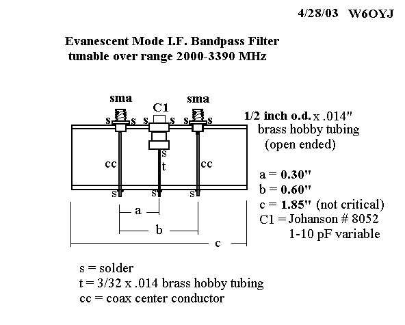
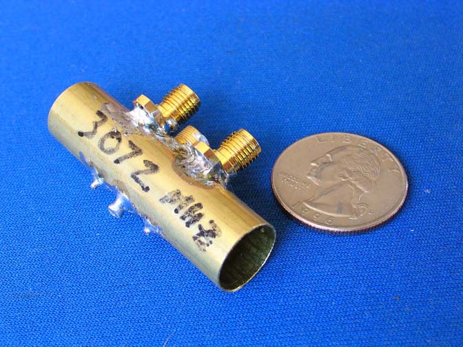
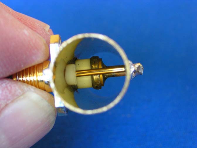
6A. New I.F. Bandpass Filters to interface between the 2-3 GHz Up/Down Converter Module and the Tx and Rx Modules. Two identical filters are needed. This filter is tunable over the 2000-3300 MHz range so it is suitable for either the Pcom Low side or High side LO modifications at 3072 or 2208 MHz respectively. The filter is made using 1/2 inch brass hobby tubing and easy to build. The tubing operates as circular waveguide below its cutoff frequency in the evanescent mode. The design is an extrapolation from the 1993 Microwave Update article by Reed Fisher, W2CQH, which used rectangular waveguide. See Photo A, and Photo B.
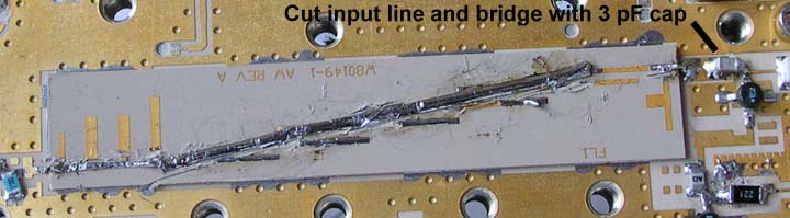
7. Modified Tx Module. The LO input and LO Doubler stages do not require retuning as they are close to their original frequencies. The i.f input attenuator device is removed and replaced with a fixed-gain ERA-3 MMIC. The i.f filter must be bypassed by soldering over it a straight piece of 50-ohm width stripline, and using an Xacto knife to carefully remove any protruding pieces of the original filter elements. A dc blocking cut is made across the input line to the right of the filter. A new 3 pF chip cap is bridged across this cut. A close-up photo shows these changes. The most difficult part of this overall project is the stripline retuning of the 22 GHz Tx drivers and amplifiers following the mixer output. That will be described in more detail in a future amendment to this status report. Currently Kerry believes two of the driver stages are contributing zero gain while one driver and the PA did respond to retuning. The current best Tx output he has achieved from the overall ODU is +18 dBm. He intends to pursue this area further. Power requirements are +12 Volts dc on transmit (12T), +5 Volts dc on transmit at 0.5A (5T), continuous -5 Volts bias (-5TR), and ground. Note: The variable gain control voltage required by the original Tx Module is not needed in the modified unit. In this modified module only four wires are used for power connections: Black for Ground, Red for +12V, Green for -5V Bias, and Yellow for +5V to the PA stages. All other original power and interface wires wires are removed.
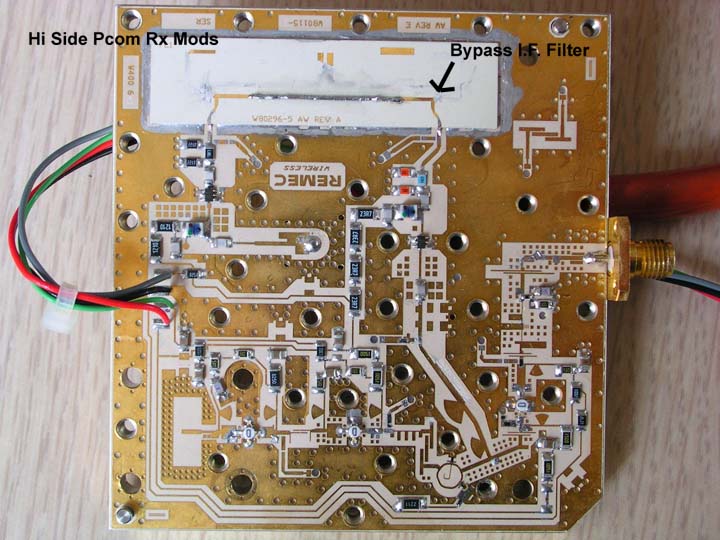
8. Modified Rx Module. No changes are needed in the LO input and LO Doubler stages. No changes or retuning are needed in the 23 GHz LNA stages ahead of the 1st mixer. The i.f. filter following the mixer is bypassed with a straight piece of 50-ohm width stripline and the residual i.f. filter elements are carefully removed with an Xacto knife. The 24 GHz receiving performance of the modified unit appears to be excellent and nearly identical to the original unit at its 23 GHz frequency. Power requirements are +12 Volts on receive (12R) (Red wire); continuous -5 volts bias (-5TR) (Green wire), and Ground (Black wire). All other original power and interface wires are removed, so only three power wires are used in this modified module.
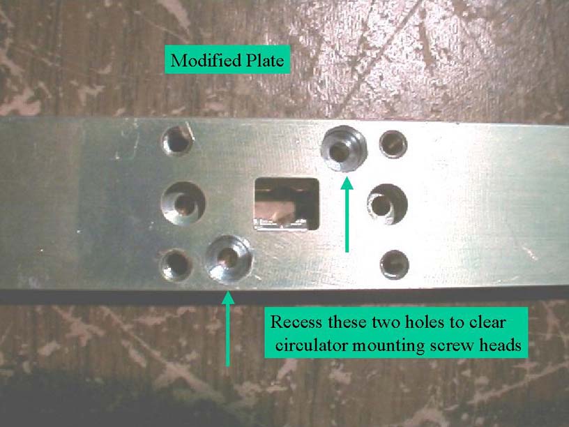
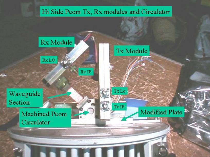
9. Antenna Interface/RF Filter/and Modified ODU Mounting Plate. The 22/23 GHz waveguide RF filter in the original Pcom ODU is not used in this High Side LO conversion. Kerry found that the TX and Rx amplifiers at the 26.4 GHz LO frequency, and the 28.6 GHz image frequency are so lossy that no filter is needed. A circulator is used to provide the T/R isolation at 24 Ghz between the Tx and Rx Modules and the dish antenna. Kerry obtained a 24 GHz circulator, machined by Chuck Swedblom WA6EXV from one of the original Pcom 23 GHz isolators. A short piece of WR-42 waveguide is used to mount the Rx Module to the circulator, which itself is bolted directly to the Tx Module and a modified antenna mounting plate. A photo of these parts of the modified ODU assembly is shown. The modified circulator has its Rx port mounted at 45 degrees to the other sides of the circulator. A rectangular cube-shaped circulator could be used instead with an appropriate short section of WR-42 or a waveguide elbow.
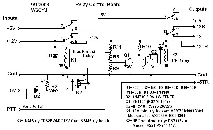
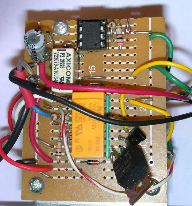
10. T/R Switching and i.f. in/out circuits. A new Tx/Rx relay control
circuit with bias failure protection is shown in the drawing. A hard
wired prototype has been built and tested but no pcb design exists at this time.
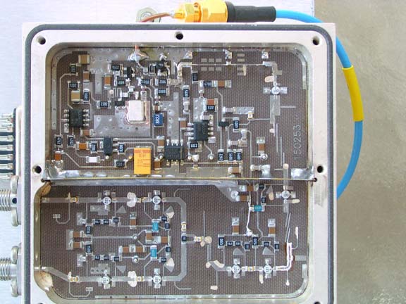
A prototype circuit of a power distribution board was also
designed and tested, with similar status. See its photo, mounted
back-to-back with the relay control board. This board uses small Molex connectors
to mate with the original cables from the Pcom Tx and Rx Modules and the modified
Pcom Synthesizer, and new cables from the TCXO, Qualcomm Synthesizer and U/D converter
board.
Tx drive level testing of the modified Pcom showed that the 1 dB
compression level for +17 dBm Tx output occurred with approximately -16 dBm of 432
MHz input to the U/D Converter board. As mods to the TX Module are not complete or
fully documented, this level should be considered as a very rough estimate. The Rx
performance of the completed system seemed to be very good, although no sensitivity
measurement has been made. The noise output of the 432 MHz i.f. transceiver increases
by about 15 dB when the dc power is applied to the Pcom ODU. These tests were made
using an external i.f. T/R switching unit.
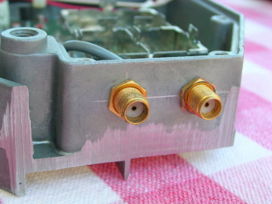
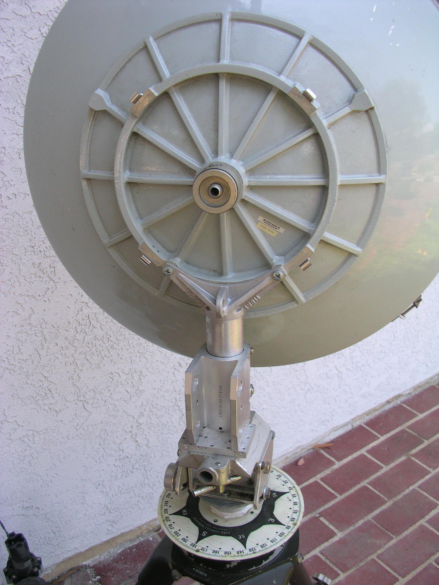
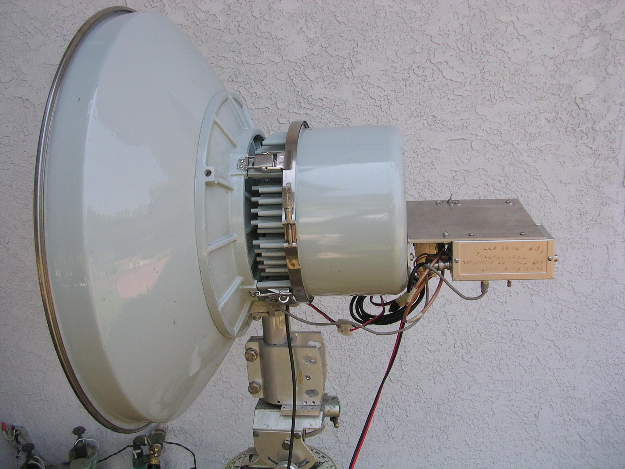
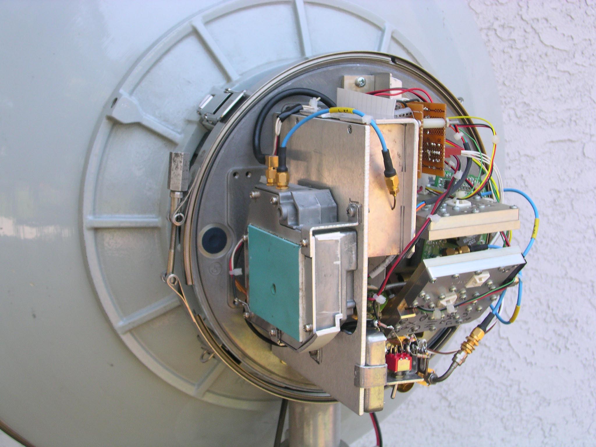
11. Pcom Antenna Configuration.
PhotoA shows a back view of the 24 inch diameter Pcom antenna
without the ODU installed. This antenna is fed via a short section of cylindrical
wavegide that engages the output of the ODU. The ODU is mounted to the back of the
antenna at four points with spring held clamps. It can be mounted in any of four
polarity orientations as the antenna feed inside the antenna assembly is symmetrical.
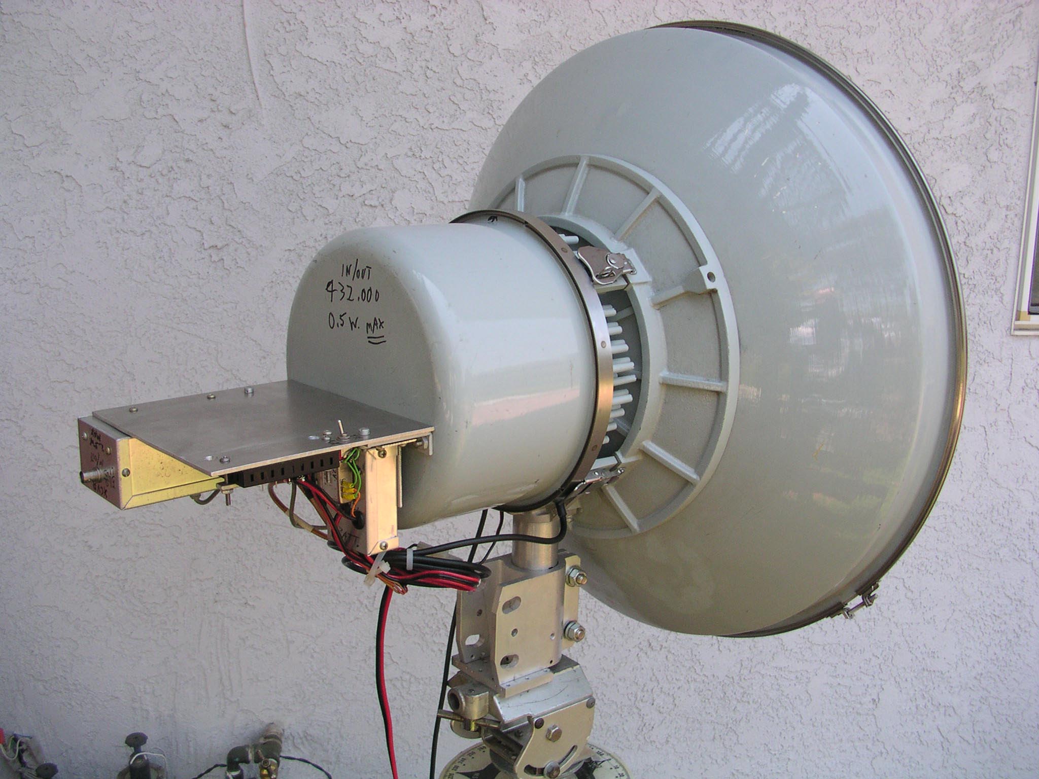
The following photos with the ODU installed are for horizontal polarization. PhotoB
shows the assembled antenna/ODU from the left side, with a platform attached to the
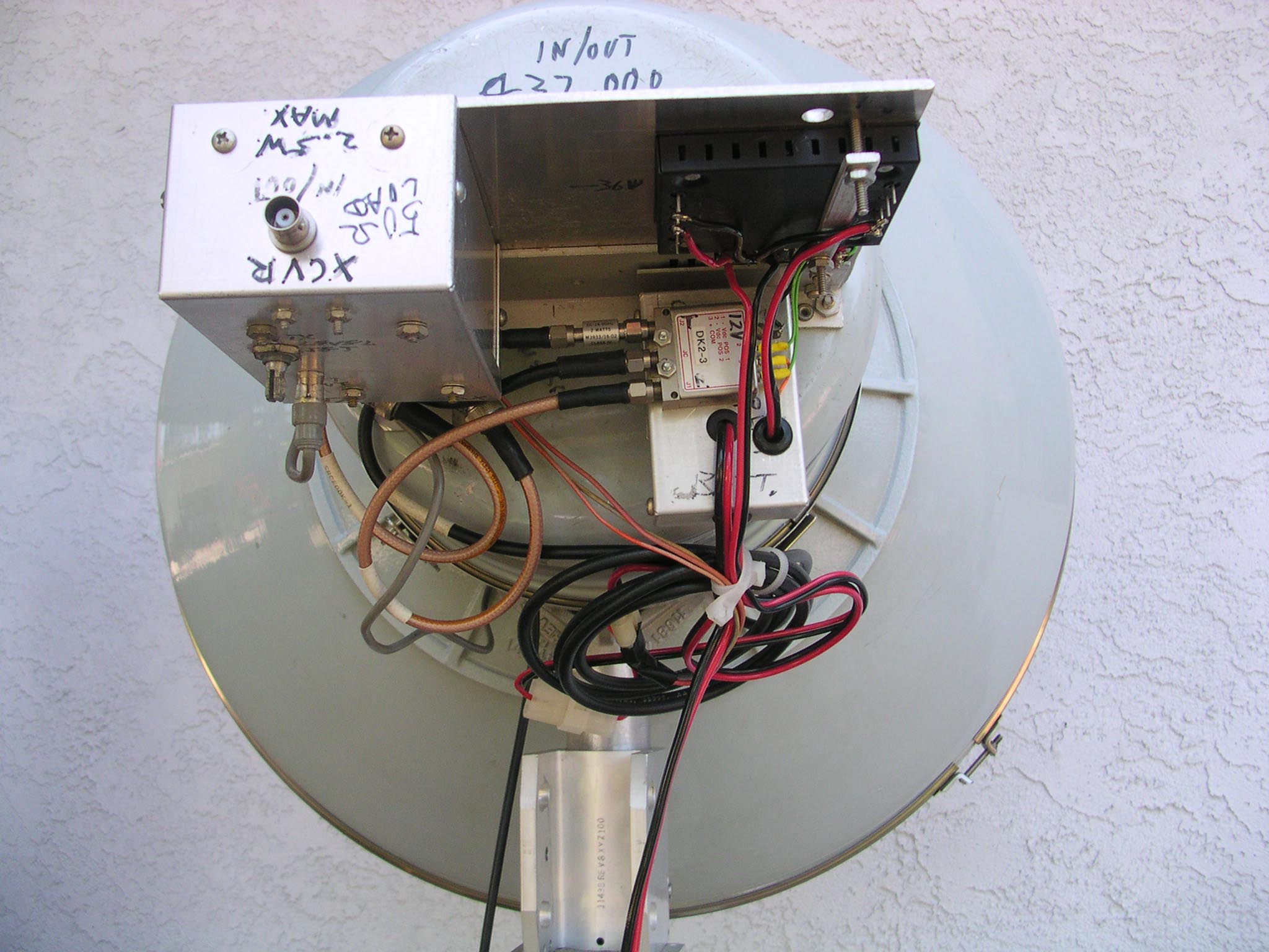
back of the ODU cover. My platform supports the i.f transceiver (on the top), and
dc-dc power converter and i.f signal Tx/Rx signal splitter (underneath). PhotoC
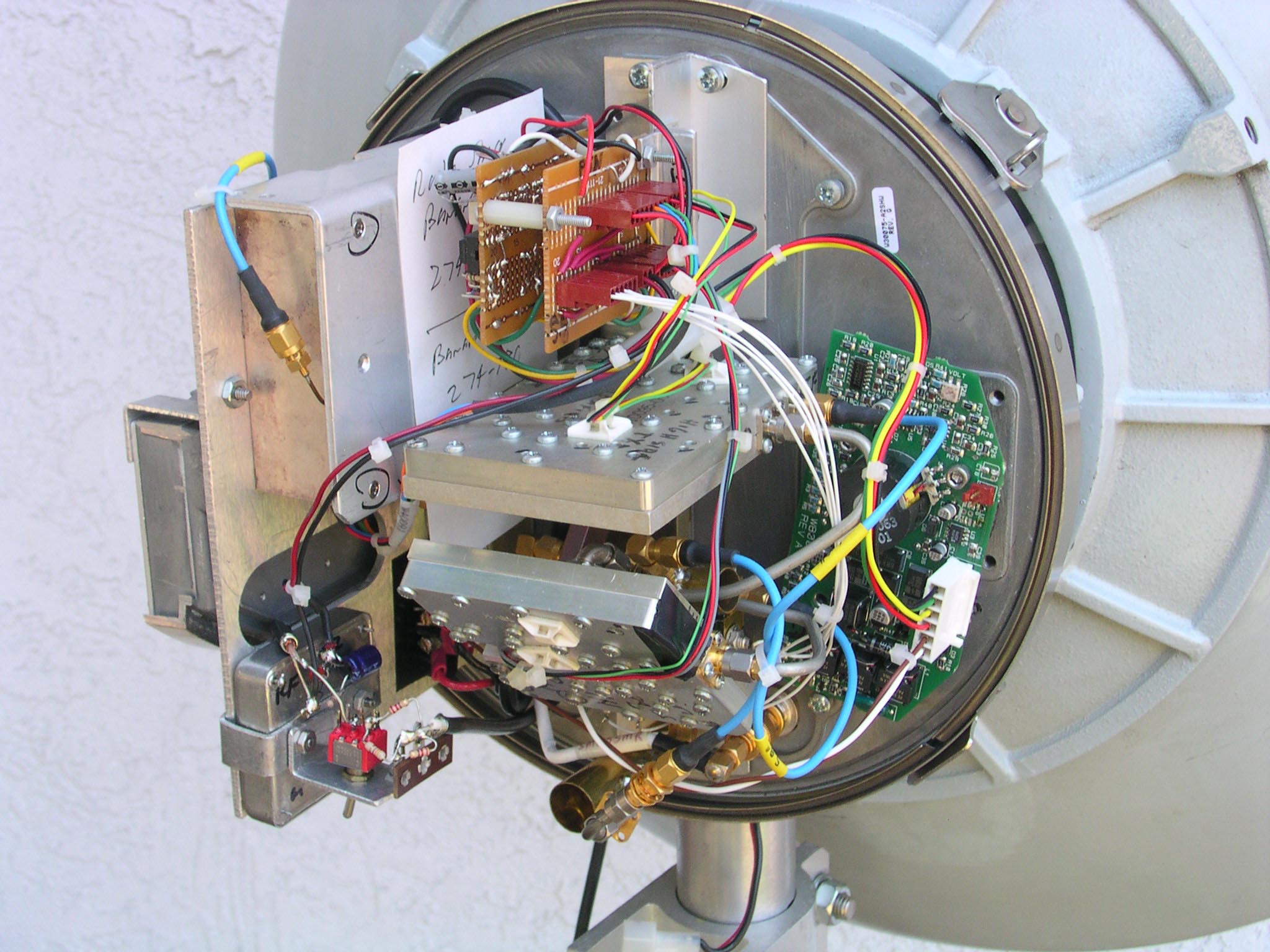
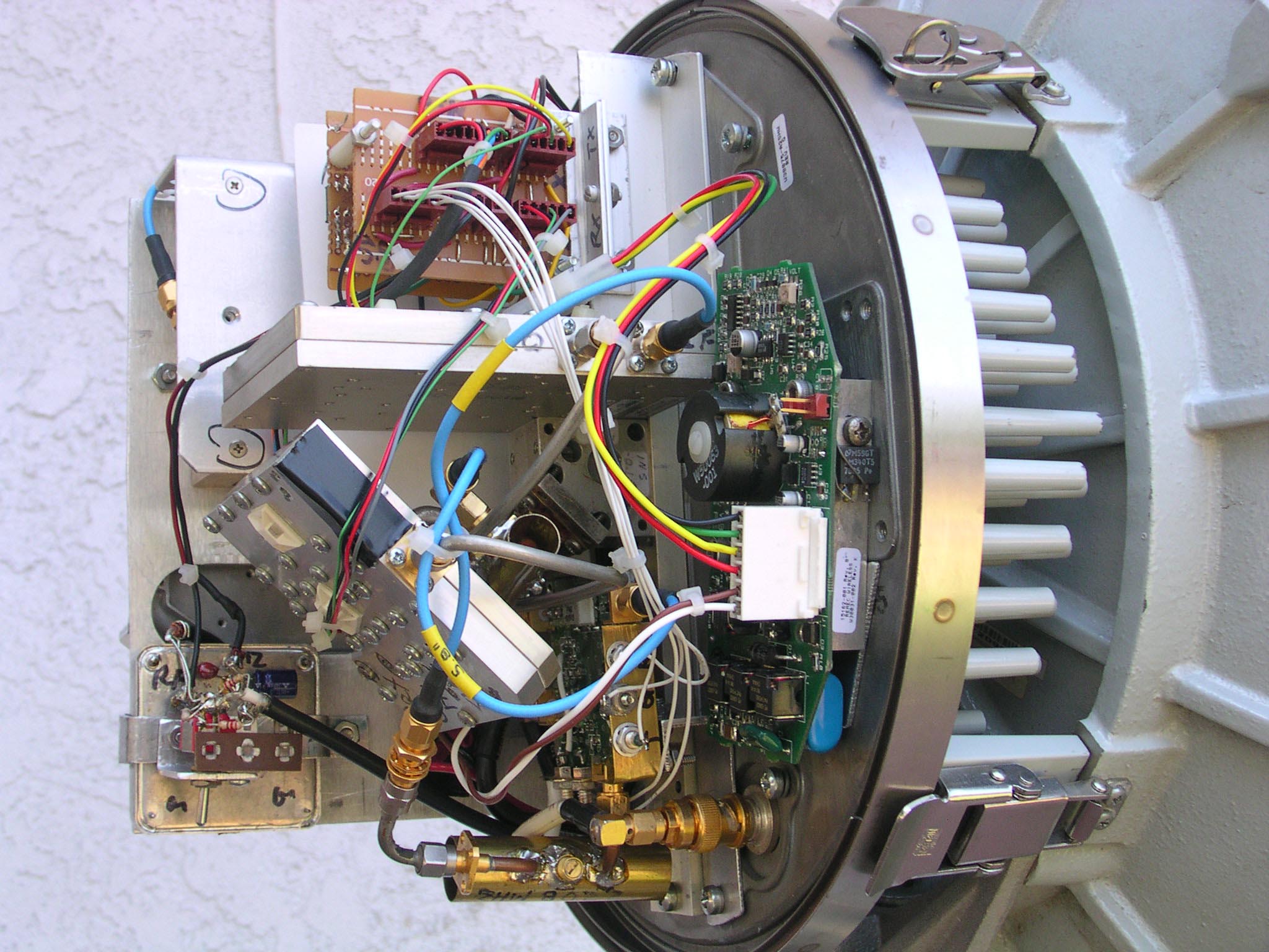
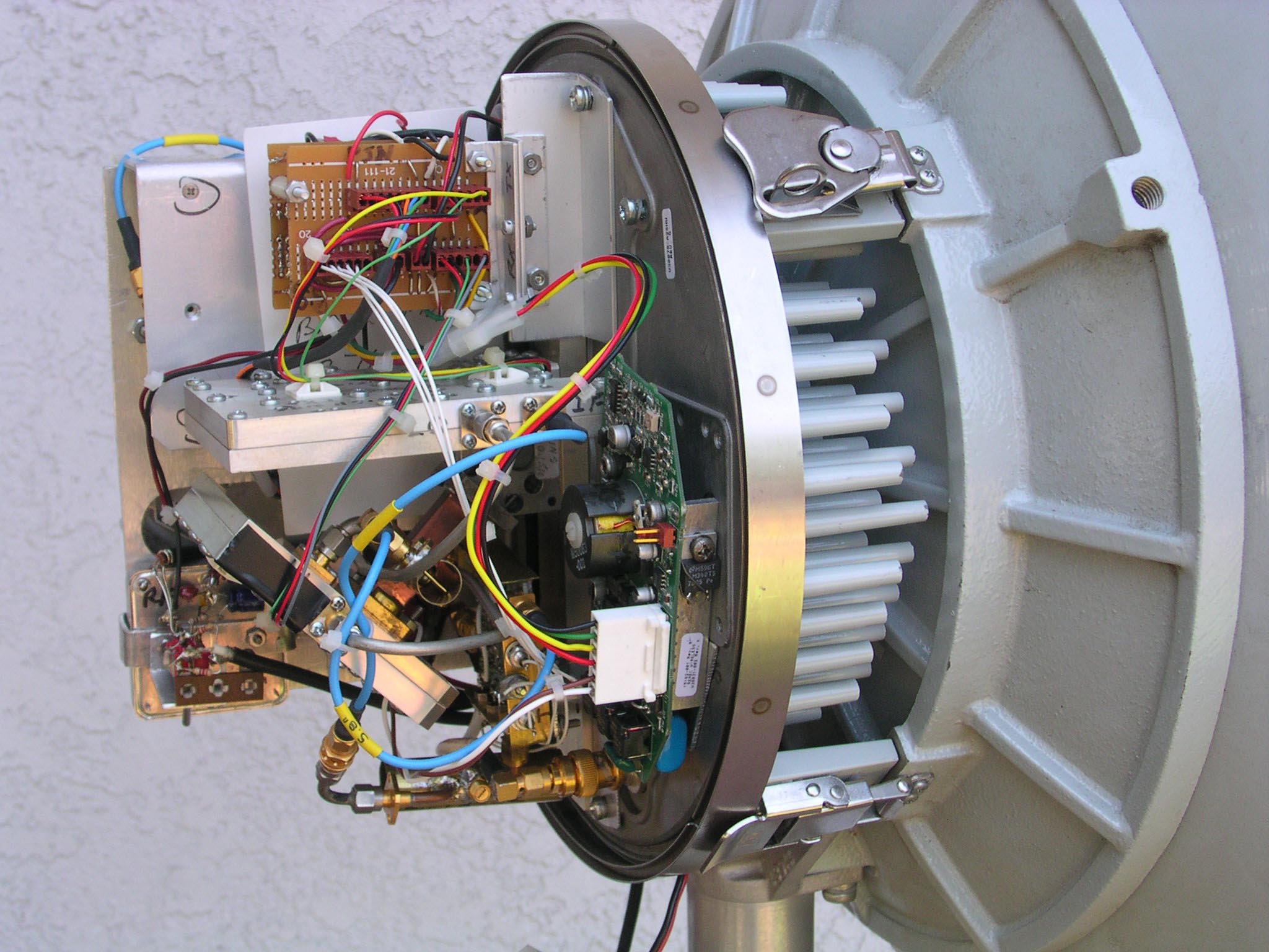
shows the assembled system from the right side. PhotoD
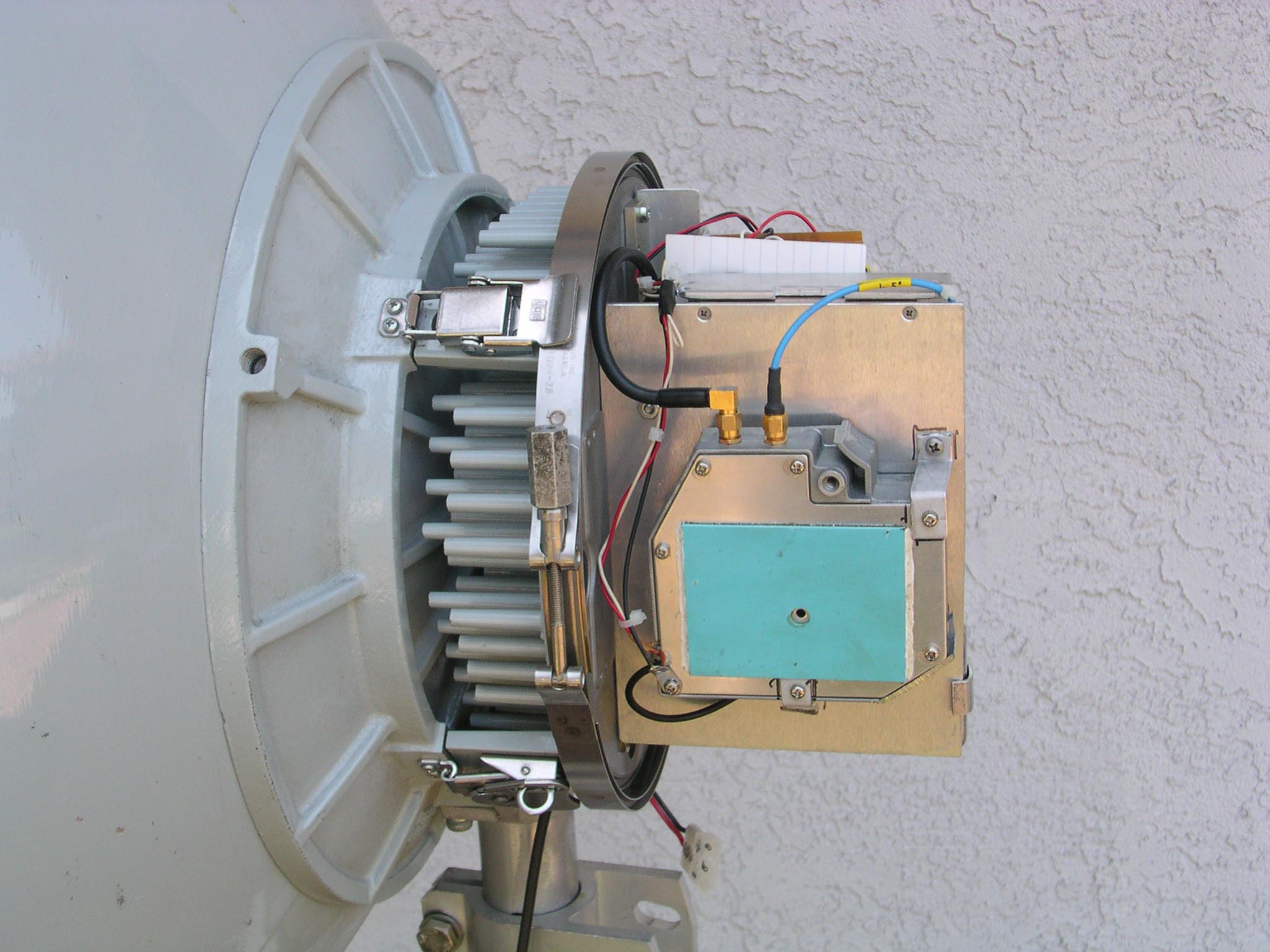
shows the view under the platform. With the ODU cover removed, PhotoE
shows the left side view of the modified ODU with the Qualcomm synthesizer mounted
vertically. The TX module and the RX module come into view in PhotoF,
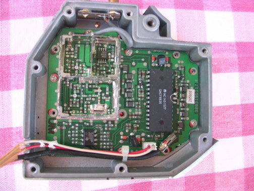
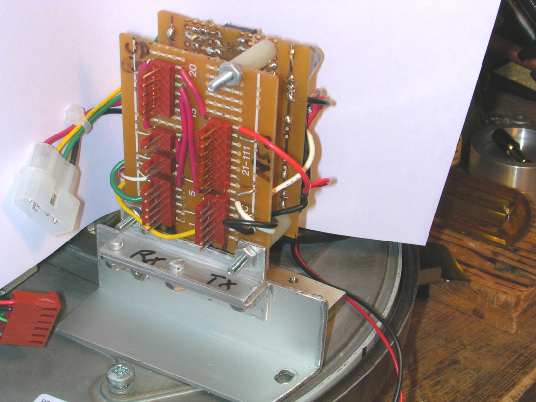
along with the Pcom Synthesizer. PhotoG shows the relay
and power distribution boards at the top, the power supply at the right,and the TX
and RX modules. PhotoH shows a closer view of the TX and RX
modules and the 2-3 GHz Up/Down converter (mixer board) nestled vertically to the
right of the RX module. One of the two 2208 MHz filters is located above the right
side of the RX module. The other filter is laying horizontally at the bottom of the
photo. Another view from the right side is shown in PhotoJ.
This concludes the status report. Further details will be furnished when available.