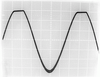
Fig. 1 Detected sine wave
Modulation acceptance is the maximum modulation level an AM receiver's detector can handle without distortion. An ordinary diode detector can accommodate upward modulation well beyond 100%. But capacitive loading can prevent a detector from faithfully reproducing downward modulation. At some point it stops and clips the waveform instead of continuing toward zero.
Fig. 1 Detected sine wave
Fig. 1 shows the output of a diode detector for a 100% amplitude-modulated sine wave. The trace is inverted because the detector circuit is arranged to generate a negative output voltage for AVC. 0 V, corresponding to no carrier, is at the top of the screen. The modulation acceptance of this detector is 88%.
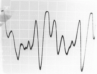
Fig. 2 Detected broadcast signal
Clipping distortion on sine waves is easily audible. In fact, you can hear it before you can see it on a scope. But casual tests suggest that clipping on speech and music isn't objectionable as long as the modulation acceptance is greater than about 80%. Fig. 2 shows an AM broadcast signal demodulated and clipped by the diode detector. While the sine wave distortion was obvious, it's not clear from the trace alone whether the broadcast waveform is distorted. In this case the ear agreed with the eye. I was listening to the receiver when I took the photo and I heard nothing amiss.
Modulation acceptance somewhere in the low-80% range is typical of consumer radios from the 1930s and 1940s. But the communications receivers I've tested have been much worse, typically distorting at 60% downward modulation or less. Distortion at such shallow modulation depths is nearly always audible. The audio tends to lose its crispness and clarity, and in severe cases sounds downright grungy. I always modify any receiver I restore for a modulation acceptance of at least 90%; most approach 100%.
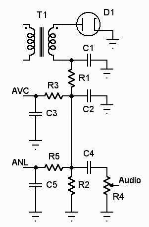
Fig. 3 Typical detector
Fig. 3 shows a typical AM detector circuit in a communications receiver. Diode D1 conducts whenever the voltage across it is positive. When the top terminal of IF transformer T1 goes positive with respect to the lower terminal, D1 clamps the terminal near ground. The lower terminal then charges C1 negatively to the waveform peak. C1 partially discharges while the IF waveform reverses sign. R1 and C2 filter out the IF component, leaving a DC level corresponding to the carrier and audio corresponding to the envelope modulation across detector load R2.
The primary cause of low modulation acceptance is back-biasing of D1 due to capacitive loading. The AVC capacitor, the volume control coupling capacitor, and any ANL capacitor are the culprits. Focus on the AVC capacitor alone to see how the damage is done.
AVC capacitor C3 charges to the level of the carrier, and the voltage on it divides back through R3 to R2. R1 and C2 are absent in some receivers, and it simplifies analysis to assume that R1, typically 47kΩ, is zero. In this case the DC voltage on R2 appears at the lower terminal of T1. Now assume that R3 is 2.2MΩ, R2 is 470kΩ, and the detected carrier level is −6 V. Under these conditions a DC bias of about −1 V appears at the lower terminal of T1 due to C3, since R2 ⁄ (R2 + R3) is about 1 ⁄ 6. When the signal drops to about one-sixth of its unmodulated level at 83% downward modulation, it generates +1 V across T1. Added to the −1 V at the lower terminal, this yields 0 V at D1. D1 stops conducting. It becomes back-biased and remains nonconducting for deeper downward modulation. R2 just sits at the −1-V bias level. This creates a flat spot in the detected waveform. The detector has clipped and distorted the demodulated audio.
If you swap R4 and C4, which leaves their current unchanged, you can see that the volume control and its coupling capacitor develop back-bias in the same way. An ANL circuit typically connects an additional filter, represented here by R5 and C5, to the detector load. This is yet another source of back-bias for D1. In each case the value of the offending capacitor matters little. These RC circuits are designed to pass or filter most of the audio spectrum, so the capacitors develop little AC voltage across them. You can think of them as little batteries. What matters is the ratio of the detector load R2 to the parallel combination of resistors that connect to these capacitors. Voltage division by this resistive divider is what causes the back-bias on D1. You can increase modulation acceptance by reducing the resistor ratio.
This analysis ignores the IF passband shape, IF source impedance, and the rectification efficiency of real diodes. These factors actually may increase modulation acceptance by lowering the effective modulation depth at the detector. However, detector back-bias usually swamps these factors in practical circuits. See the detection section of Frederick Terman's Radio Engineers' Handbook for more.
AVC resistor R3 typically is 2.2MΩ. I've increased its value to 4.7MΩ without problem. If you try this, it's a good idea to check for leakage current in the AVC circuit, particularly when several tubes are controlled. Any leakage current develops an offset voltage across R3; doubling R3 doubles the offset. Increasing R3 will lengthen the AVC time constant, but I've found that the AM time constant is way too short in most receivers, so this normally is not a problem. You can decrease C3 to compensate if you want.
Some communications receivers (and most consumer radios) replace R2 with the volume control R4, typically 500kΩ. C4 then connects the wiper to a grid resistor, typically 10MΩ. Because this AC-coupled load has much higher resistance than the volume control, this circuit configuration can greatly improve modulation acceptance. This technique applies DC from the detected carrier to the volume control. If the wiper contact is worn or dirty, rotation can generate interrupted DC, causing scratchy audio noise. Make sure the volume control is in good condition if you try this circuit.
R5 typically is 1MΩ. This resistor, along with another 1MΩ resistor often used in series-ANL circuits and not shown, can be major contributors to poor modulation acceptance. There is a way to eliminate the R5-C5 network and any additional resistor, and use the AVC capacitor for the ANL function. Not only does this modification improve modulation acceptance, it makes ANL so transparent that you can leave it permanently engaged. It also automatically implements fast-attack AVC, which helps if you modify your AVC system to minimize selective-fading distortion.
An alternative way to improve modulation acceptance is to use a separate diode for detecting AVC and ANL, leaving the existing diode for audio detection only. The second diode in a 6SQ7, for example, is often unused (or tied in parallel with the first diode). If you couple the anode of D1 to the anode of a second diode through 100 pF or so, you can connect the AVC and ANL resistors to the new diode, along with a second load resistor. D1 is then DC-isolated from the AVC and ANL capacitors, and only the volume control coupling capacitor can degrade modulation acceptance. Better still is to connect the 100 pF directly to the plate of the last IF amp. This feeds a wider passband to the AVC detector and keeps it from boosting the gain as you tune away from a station, eliminating raucous noises. The coupling capacitor must have low leakage if tied to the IF-amp plate. Because of the high-level IF signal at D1, you must take care any time you modify its wiring. Unwanted coupling can result in IF feedback that may alter the gain and frequency response of the IF strip, or even cause it to oscillate.
 88–108 MHz
Originally published in Electric Radio, August 2003